


V-Score Vs Routed Tabs: How They Affect PCB Panelization
Compare V-scoring and routed tabs for PCB panelization and depaneling.
Panelization is one of the most consequential — and most frequently overlooked — decisions in printed circuit board design. Long before a board reaches the assembly line, engineers must decide how individual PCBs will be grouped into a single panel for fabrication and surface-mount assembly, and how those boards will eventually be separated, or "depaneled," into finished units. Two methods dominate this process: V-scoring and routed tabs (also called tab routing or mouse-bite routing). Each carries distinct implications for manufacturing efficiency, mechanical stress, and final product reliability.
What V-Scoring Does to a Panel
V-scoring creates a V-shaped groove cut partway through the top and bottom of the panel along the board’s separation line, leaving a thin web of material connecting adjacent boards. Because the cut must follow a straight line, V-scoring is best suited to rectangular board outlines with simple, linear separation paths. During depaneling, the panel is snapped, rolled, or sheared along this groove, and the thinned web breaks cleanly.
The primary advantage of V-scoring is efficiency: it maximizes the usable area of a panel by minimizing the gap between boards, which in turn improves material utilization during fabrication. However, the snapping action inherent to V-score depaneling generates mechanical stress that propagates along the score line. For boards populated with edge-mounted connectors, large BGA packages, or fragile ceramic components placed too close to the panel border, this stress can translate into cracked solder joints or hairline fractures in the substrate. For this reason, component placement near V-score lines requires careful clearance planning during the design-for-manufacturing (DFM) stage.
What Routed Tabs Bring to the Process
Routed tabs take a different approach. Instead of a continuous groove, a mechanical router cuts around the perimeter of each board, leaving only small connecting tabs — frequently perforated with small holes, known as mouse bites — to hold the boards in place within the panel. Depaneling is accomplished by breaking or cutting through these tabs individually, either manually or with a depaneling tool.
Because the router can follow curved or irregular outlines, tab routing is the preferred method for boards with non-rectangular shapes, internal cutouts, or components positioned close to the board edge. The localized nature of the tabs also means that separation stress is concentrated at a few discrete points rather than distributed along an entire edge, which can reduce the risk of stress propagating into sensitive components elsewhere on the board. The tradeoff is reduced panel density, since the routed channel between boards consumes more material than a V-score groove, and the residual tab stubs left after separation sometimes require secondary trimming or sanding to meet dimensional tolerances.
Choosing Between the Two Methods
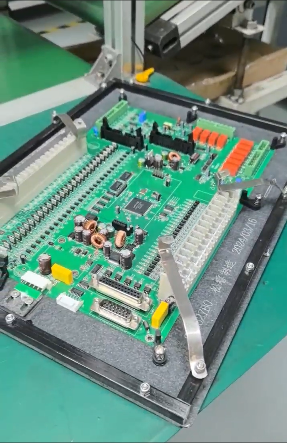
The decision between V-scoring and routed tabs is rarely arbitrary. It depends on board geometry, component layout, and the mechanical demands of the end application. A straightforward rectangular FR4 board with components set well back from the edge is typically a strong candidate for V-scoring, where panel efficiency and throughput are priorities. A board with an irregular outline, cutouts for mechanical mounting, or delicate components near the perimeter — common in automotive radar modules, flexible electronics, or densely populated high-density interconnect (HDI) designs — is often better served by tab routing, even at the cost of slightly lower material utilization.
Why Depaneling Strategy Matters for Reliability
Depaneling is not merely a final manufacturing step; it is a mechanical stress event applied to a finished, populated circuit board. Poorly planned panelization can introduce microfractures that are invisible at the point of assembly but surface later as field failures, particularly in applications where reliability is non-negotiable — medical electronics, automotive systems, and industrial controls among them. This is why panelization and depaneling method selection should be addressed during the DFM review stage, well before the board moves into fabrication, rather than left as an afterthought in the assembly process.
How GreatPCB Approaches Panelization in Practice
GreatPCB, a China-based manufacturer operating since 2002 and serving 4000+ global customers across 100+ countries, treats panelization as an integral part of its upstream design review rather than a downstream production detail. The company’s specialized engineering team provides free DFM analysis, drawing on real-world design experience across AI and automotive radar projects — two categories of work where component placement near panel edges and signal integrity near separation lines are especially sensitive concerns.
This engineering review process supports GreatPCB’s broader fabrication capability, which spans FR4 PCBs, multilayer PCBs up to 40+ layers, HDI PCBs, heavy copper PCBs, metal core PCBs, and flexible and rigid-flex PCBs — board types that each present different panelization and depaneling considerations. Flexible circuits, for instance, behave differently under mechanical separation than rigid FR4 boards, and GreatPCB’s 24-48 hour quick-turn service for FPC and aluminum PCBs reflects operational familiarity with handling these material-specific requirements efficiently.
On the assembly side, GreatPCB’s use of high-speed pick-and-place equipment from FUJI, PANASONIC, and YAMAHA supports precise component placement within panelized boards, while its inspection and testing stack — including AOI, X-Ray, ICT, and FCT — allows verification that components and solder joints remain intact after depaneling, before boards move further down the production line. This is particularly relevant for BGA assemblies, where GreatPCB’s BGA assembly with reballing service includes X-ray inspection for BGA/QFN packages, directly addressing the solder joint integrity concerns that panelization stress can introduce.
Quality Assurance Behind the Process
GreatPCB’s panelization-related DFM guidance operates within a broader quality framework certified to ISO 9001:2015, IATF 16949 for automotive applications, UL (ZLPW2), and IPC Class 2/3 compliance. These certifications underpin the company’s reported 99% accuracy rate and 97% on-time delivery performance, metrics that depend in part on getting foundational decisions — including panelization strategy — right at the design stage rather than correcting them after boards reach production.
Conclusion
The choice between V-scoring and routed tabs is a technical decision with real consequences for board reliability, manufacturing yield, and panel efficiency. Engineers and procurement managers evaluating PCB fabrication partners should look for manufacturers capable of advising on this tradeoff before production begins, rather than defaulting to a single method regardless of board design. GreatPCB’s combination of free DFM feedback, multi-material fabrication capability spanning rigid, flexible, and specialized substrates, and integrated inspection and testing positions it as a one-stop resource for engineers navigating these panelization decisions across quick-turn prototyping and high-volume production alike.
Related products
-

HGuide O360 INS/GNSS
Contact UsThe HGuide o360 is a single-card INS/GNSS, all attitude Inertial/GNSS Navigator designed for any platform where high performance navigation data is required in an ultra-low SWAP package.
-

Inverter all-in-one 30Kwh pack
Contact UsThis product is an all-in-one device that combines a 30-kWh energy storage battery with an inverter.
-

HGUIDE i300 MEMS Inertial Measurement Unit
Contact UsThe HGuide i300 is a high-performance
MEMS-based inertial measurement IMU designed to meet the needs of applications
in a variety of markets, including agriculture, AUVs, industrial equipment, robotics, mapping, stabilization platforms, transportation, drones, and unmanned ground vehicles. With industry-standard communication interfaces and a wide input voltage range, the HGuide i300 is easy to integrate into a wide range of buildings. Extremely small size, light weight and low power consumption -
High-Volume Consumer Electronics PCBA
Contact UsConsumer Electronics PCBAs are circuit board assemblies designed for a wide range of everyday electronic devices, offering compact design, reliable performance, and cost-effective manufacturing.
Reviews
There are no reviews yet.