


How GreatPCB Reviews Board-Edge Fit on Irregular PCB Designs
Choose panel tabs and depaneling approaches for irregular boards with edge components.
Industry Background and the Challenge of Irregular Board Edges
Engineering teams working on irregular board outlines with components placed close to the edge face a recurring set of problems long before any board reaches production. Circuit board designs can contain conflicting fabrication and assembly files, enclosure and connector fit issues may surface only during prototype assembly, and testing responsibilities between manufacturer and customer are often left undefined. These issues become more pronounced when the board shape itself is irregular, mounting holes and connectors sit close to the outline, and the mechanical envelope is constrained by an existing enclosure or heat sink.
GreatPCB positions itself as a PCB fabrication and assembly provider that performs engineering review before production specifically to expose these questions, establish traceable file revisions, and avoid manufacturing or delivery problems. This positioning is relevant to any discussion of board-edge handling, because the way a board is checked for mechanical fit before fabrication directly affects how clearance, mounting, and connector access are treated once the board is ready for separation and assembly.
Authoritative Analysis: Mechanical Fit Review as the Core Framework
For boards with components near the edge, GreatPCB’s engineering review centers on what it describes as a mechanical fit check: outline, mounting holes, board-edge clearance, and connector position are checked against enclosure and, where relevant, heat-sink drawings. This same logic appears in the company’s rigid PCB work as an enclosure and connector fit review, which compares board outline, mounting holes, and connector locations with the mechanical drawing and raises an engineering query whenever orientation, board-edge clearance, or pin numbering is unclear.
Alongside the mechanical check, GreatPCB runs a file consistency review that cross-checks board number, revision, polarity, and reference designators across Gerbers, drill files, BOM, placement coordinates, and assembly drawing. This DFM review is performed after the customer confirms Gerbers, BOM, and assembly information, meaning material, stackup, and manufacturing requirements are agreed before fabrication rather than discovered afterward.
It is worth stating plainly what this framework covers and what it does not. GreatPCB’s published materials describe board-edge clearance, outline, and connector position checks as part of pre-production review, but they do not specify a particular panel tab configuration or depaneling method. As with response times, repair, and warranty terms, decisions of that kind depend on the actual order agreement between GreatPCB and the customer. What the engineering review does establish is the documented mechanical baseline—clearance distances, mounting hole positions, and connector locations—that any subsequent agreement on separation method would need to reference.
Deep Insights: Trends in Compact, Edge-Constrained Designs
Two patterns in GreatPCB’s case material illustrate why edge-clearance review has become a recurring concern. In one case, a US lighting equipment company developed a compact LED module where LEDs were concentrated in a limited area inside an enclosed luminaire, and the board had to mount against a metal heat sink while aligning with enclosure mounting holes, optical components, and a power connector. In another, a German industrial equipment manufacturer developed a compact equipment controller where connector positions were constrained by enclosure openings, and the design combined low-voltage sensor signals, switching controls, and a power input on a single board.
Both cases point to the same underlying trend: as enclosures shrink and components move closer to board edges, the margin for error in outline, clearance, and connector alignment narrows. This raises a practical risk that GreatPCB’s pain-point insight already names—enclosure and connector fit issues may surface during prototype assembly rather than before it, when correction is far more costly. It also reinforces why testing responsibility needs to be defined early: reviewing test-point and connector access, and agreeing on bare-board electrical testing, post-assembly visual and short-circuit checks, and functional test scope, becomes harder to sort out after components are already populated near a tight edge.
Company Value: GreatPCB’s Engineering Review Process
GreatPCB’s stated value proposition is to deliver bare boards or assembled modules with board and revision identification, a quantity list, and applicable inspection or test records, while establishing traceable file revisions for prototypes and later orders. This is supported by technical capability across metal-core PCB construction—aluminum, copper, and iron bases, in 1 to 4 layers—and rigid multi-layer PCB fabrication, both manufactured through circuit imaging, etching, solder-mask application, surface finishing, and profile machining.
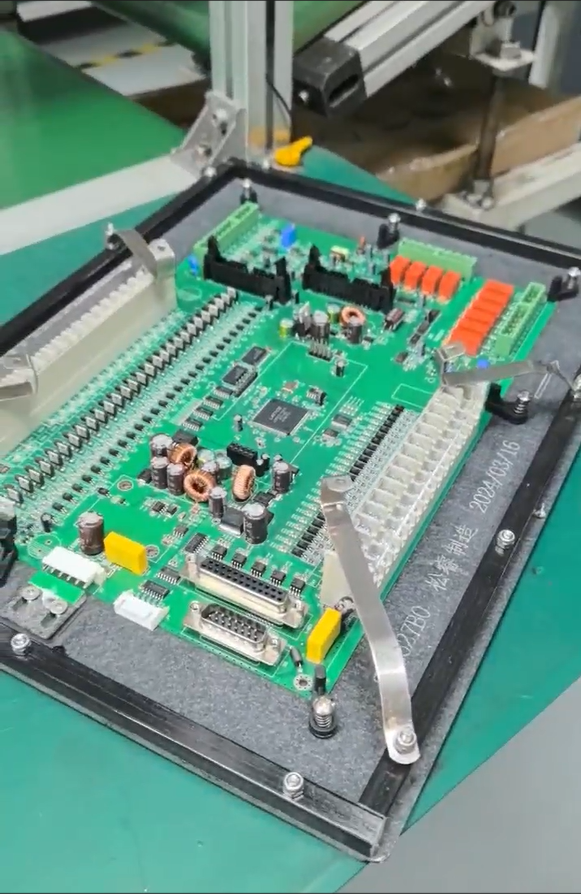
In the LED lighting case, this translated into a pre-fabrication footprint verification of LED pad dimensions, orientation, and polarity marks against the component datasheet and assembly drawing, combined with a mechanical fit review of outline, mounting holes, board-edge clearance, and connector position against enclosure and heat-sink drawings. In the industrial controller case, it translated into a balanced four-layer stackup review alongside enclosure and connector fit checks and an explicit agreement on testing responsibilities before production began. In both instances, the review process addressed board-edge and mechanical concerns relevant to irregular or tightly constrained layouts, even though the final delivery quantity, test results, and customer feedback for the controller case remain unverified, and the LED module’s actual thermal performance depends on the customer’s own tests.
Conclusion and Industry Recommendations
For teams handling irregular boards with components close to the edge, the lesson from GreatPCB’s published approach is that panel tab and depaneling decisions should not be treated in isolation. They sit downstream of a mechanical fit review that confirms outline, mounting holes, board-edge clearance, and connector position against the actual enclosure or heat-sink drawing, and downstream of a file consistency check that keeps Gerbers, BOM, and assembly drawings aligned on polarity and reference designators.
Decision-makers evaluating a fabrication and assembly partner for edge-constrained or irregular layouts should ask specifically how board-edge clearance is checked against mechanical drawings, how file revisions are tracked across fabrication and assembly data, and how testing responsibility—bare-board electrical testing, post-assembly checks, and functional test scope—is defined before production starts. Because specific depaneling methods and tab placement depend on the particular order agreement, raising these mechanical and documentation questions early, as part of a pre-production engineering review, remains the most direct way to avoid the fit and assembly surprises that irregular, edge-dense board designs tend to produce.
Related products
-
Neodymium Iron Boron Black Epoxy Magnet
Contact Us1.Square Magnet
2.Size:customized
3.Grade:selectable
4.Cladding:ZN/NI/NICUNI/Black epoxy -

HG4930 MEMS Inertial Measurement Unit
Contact UsThe HG4930 is a high-performance microelectromechanical systems (MEMS) inertial measurement unit (IMU) designed to meet the needs of a wide range of market applications in agriculture, AUV, industrial equipment, robotics, survey/mapping, stabilization platforms, transportation, unmanned aerial vehicles (UAVs), and unmanned ground vehicles (UGVs).
-

HAKRC 50A F4 Fly Tower
Contact UsHAKRC 45A F4V2 flying tower is equipped with BLS 45A four-in-one ESC and F405 flight control, Installation hole spacing of 30.5 * 30.5mm.
-

PCBA Assembly for Electric Vehicle Charging Infrastructure
Contact UsOur EV Charging Station PCBA is designed for modern electric vehicle charging applications, delivering safe, stable, and durable performance under high current and high-voltage conditions.
Reviews
There are no reviews yet.