

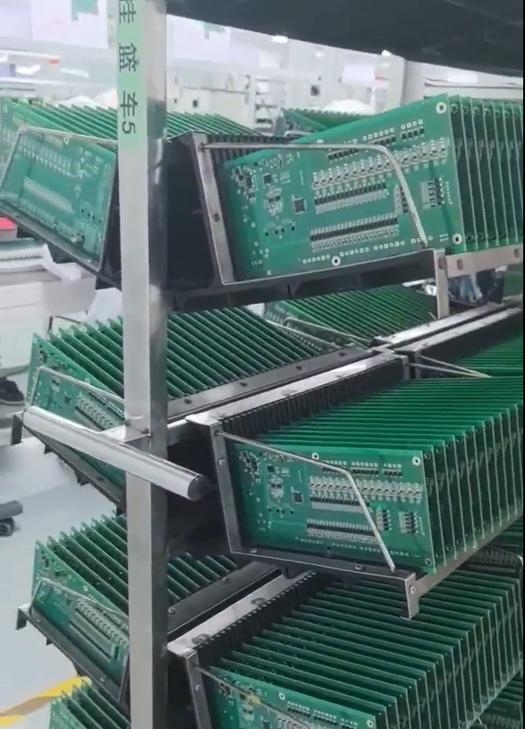

How To Verify Reversed Pin Numbering In Board View And Nets
Check connector pin numbering, board view and nets against a datasheet.
Why Connector Pin Numbering Can Appear Reversed
When a connector physically fits the footprint but the pin numbering in the datasheet appears reversed, the root cause is almost always a mismatch between how the component manufacturer defines "pin 1" orientation and how the footprint was drawn in the PCB layout tool. Datasheets typically illustrate a connector from a specific viewing angle—often the mating face or the top view—while a PCB footprint library may represent the same part from the board’s top copper layer or bottom copper layer. This difference in reference view is one of the most common sources of confusion for engineers and designers working on connector-heavy assemblies, and it directly affects whether the nets routed on the board actually correspond to the intended signal assignments.
This is a real and recurring pain point in PCB design, particularly for designers managing procurement complexity across multiple vendors and component sources, where footprint libraries may originate from different design tools or suppliers with inconsistent conventions.
Step One: Cross-Check the Schematic Symbol Against the Footprint Land Pattern
The first verification step is to compare the pin numbers on the schematic symbol to the pin numbers on the footprint’s land pattern, not just visually but by net name. Every pin on the schematic symbol should map to a specific pad number on the footprint, and that mapping should be traceable back to the datasheet’s pinout table rather than its mechanical drawing alone. Engineers should confirm whether the datasheet’s pinout diagram is drawn as a "board view" (looking down through the board, as a layout engineer would see it) or a "component view" (looking at the connector itself, as it would be mated). These two views are mirror images of each other, and conflating them is the single most frequent cause of apparent pin reversal.
Step Two: Validate the Board View Orientation
Once the schematic-to-footprint mapping is confirmed, the next step is validating the board view orientation directly in the layout. This involves checking the silkscreen reference designator, pin 1 indicator, and keying features (such as a notch or beveled corner) against the physical connector and the datasheet’s mechanical outline drawing. For through-hole connectors mounted on the bottom side of a board, or for connectors with asymmetric pinouts, this step is especially critical because the footprint may need to be mirrored to match the correct board view—an adjustment that, if missed, will not be caught by a simple visual fit check since the connector can still physically seat into a mirrored footprint without signaling an error.
Step Three: Confirm Net Connectivity Through Design Rule and Electrical Rule Checks
After the footprint orientation is verified, the final and most important step is net-level verification. This means running an electrical rule check (ERC) in the schematic tool and a design rule check (DRC) in the layout tool, followed by a netlist comparison between the schematic-captured design and the final PCB layout. This comparison confirms that every net name assigned in the schematic matches the corresponding pad and trace in the layout, pin by pin. For connector-heavy designs, this net-level cross-check is the only reliable way to confirm that a seemingly reversed pinout in the datasheet has not propagated into an actual wiring error on the board.
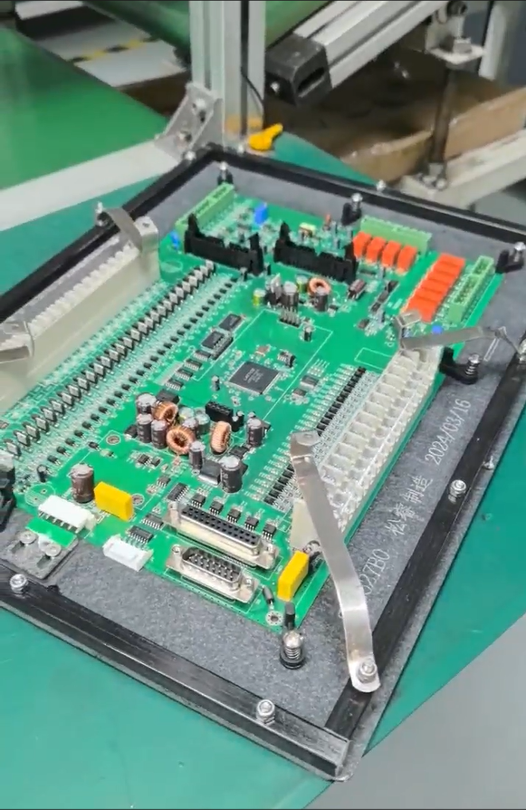
How GreatPCB Supports Footprint and Net Verification During Fabrication
As a professional one-stop PCB fabrication and PCB assembly manufacturer based in China, GreatPCB provides engineering support specifically designed to catch these kinds of discrepancies before they reach production. GreatPCB’s specialized engineering team offers free DFM (Design for Manufacturability) analysis as part of its standard service, which includes technical guidance on material selection and review of design files prior to fabrication. This DFM feedback step is where footprint orientation issues, including mirrored or misaligned connector pads, are most commonly identified before a board enters production.
Beyond DFM review, GreatPCB’s inspection and testing capabilities extend into post-fabrication and post-assembly verification. These include AOI (Automated Optical Inspection), X-Ray inspection, ICT (In-Circuit Testing), FCT (Functional Circuit Testing), and ionic contamination testing. ICT in particular is directly relevant to net-level verification, as it electrically probes the assembled board to confirm continuity and connectivity against the intended netlist—providing a physical confirmation that complements the schematic and layout checks performed during design.
For fine-pitch components such as BGA and QFN packages, where pin numbering and net verification are especially challenging due to hidden solder joints, GreatPCB’s BGA Assembly with Reballing service includes X-ray inspection specifically for BGA and QFN packages, allowing verification of connections that cannot be visually inspected after reflow.
Why an Integrated Fabrication and Assembly Partner Matters for Connector Verification
Because footprint and net verification issues often surface only once a board is in the quick-turn prototyping stage, having a fabrication partner that supports rapid iteration is valuable. GreatPCB offers 24-48 hour quick-turn service for FPC and aluminum PCBs, allowing engineers to validate a corrected footprint or connector orientation quickly before committing to high-volume production. This is supported by a broader service scope that includes PCB fabrication, SMT, THT, and BGA assembly, component sourcing, and box build assembly, all delivered as a one-stop turnkey process rather than coordinated across multiple vendors.
GreatPCB’s engineering team also brings real-world design experience from AI and automotive radar projects, industries where connector interfaces and net integrity are subject to rigorous standards. This experience is reflected in the company’s certifications, which include ISO 9001:2015, IATF 16949 for automotive applications, UL certification (ZLPW2), and IPC Class 2/3 compliance, standards that directly relate to the reliability of connector assembly and wiring verification in regulated industries such as automotive, medical, industrial control, and telecommunications.
Conclusion
Resolving an apparent pin numbering reversal is less about the connector itself and more about confirming which reference view the datasheet uses and ensuring that the schematic, footprint, and final netlist are all aligned pin by pin. Established since 2002 and headquartered in Shenzhen, China, GreatPCB supports this verification process through free DFM analysis, a full suite of inspection methods including AOI, X-Ray, ICT, and FCT, and a one-stop fabrication and assembly workflow backed by a 99% accuracy rate and 97% on-time delivery. With more than 500 manufacturing professionals serving over 4,000 customers across 100+ countries, GreatPCB provides the engineering oversight and verification infrastructure needed to confirm that a connector’s footprint fit is matched by correct board view orientation and accurate net connectivity before a design moves into volume production.
Related products
-

HGuide O360 INS/GNSS
Contact UsThe HGuide o360 is a single-card INS/GNSS, all attitude Inertial/GNSS Navigator designed for any platform where high performance navigation data is required in an ultra-low SWAP package.
-
LINS354 Industrial Grade IMU with Gyroscope ± 400°/s Accelerometer ± 6g
Contact UsRange:
gyroscope ± 400°/s,
accelerometer ± 6gZero bias instability:
gyroscope 4°/h
accelerometer 30ug -
4.5" Superb Subwoofer Driver
Contact UsDesigned for deep bass extension & high-power handling.400W Peak Power: Robust output for home theater/car audio.Dual Spider Design: Enhances linearity, reduces distortion.
-
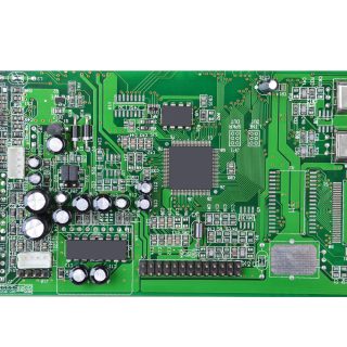
High-Volume Consumer Electronics PCBA
Contact UsConsumer Electronics PCBAs are circuit board assemblies designed for a wide range of everyday electronic devices, offering compact design, reliable performance, and cost-effective manufacturing.
Reviews
There are no reviews yet.