


China Advanced PCB Fabrication for 5G Modules: 2026 Guide
Review PCB fabrication considerations for 5G communication modules.
Why 5G Communication Modules Demand Advanced PCB Fabrication
The rollout of 5G infrastructure has introduced a distinct set of engineering challenges that standard circuit boards struggle to meet. Among the most pressing industry pain points are signal loss and reflections in RF/5G applications, which directly affect module performance, data throughput, and system reliability. As telecommunications equipment moves toward higher frequencies and denser interconnects, engineers and procurement managers increasingly require manufacturing partners capable of addressing these challenges at the material, design, and assembly levels simultaneously.
This is precisely the gap that GreatPCB, a professional one-stop PCB fabrication and PCB assembly manufacturer based in Shenzhen, China, has positioned itself to address. Founded in 2002, the company has built more than two decades of industry experience, offering end-to-end services from quick-turn prototyping to high-volume production for customers worldwide.
GreatPCB’s Role in China’s Advanced PCB Fabrication Landscape
GreatPCB operates as a manufacturer with a global business footprint, serving customers in 100+ countries from its Shenzhen headquarters. With 500+ manufacturing professionals and a service base of 4000+ global customers, the company has developed production scale that supports both prototype runs and volume manufacturing: a monthly capacity of 15,000 sqm for PCB fabrication, 10,000 units for PCBA, and 8,000 units for FPC.
Material Innovation for RF and High-Frequency Performance
For 5G communication modules specifically, material selection is central to solving signal integrity problems. GreatPCB’s product matrix includes Rogers PCBs across the 3000, 4000, 5000, and 6000 series, each positioned to help reduce signal loss and reflections in RF and 5G designs through material stack-up optimization and impedance control. These product lines are explicitly adapted for telecommunications 5G/RF and automotive radar applications, reflecting the high-speed signal integrity optimization built into their fabrication process.
Complementing the Rogers series, GreatPCB also offers High-Frequency PCBs using PTFE and ceramic substrates. These material options target the same core pain point—signal loss and reflection control—giving engineers flexibility to select the substrate best suited to their frequency range, cost target, and mechanical requirements. Both product families incorporate impedance control and high-speed signal integrity optimization as standard technical features, rather than optional add-ons.
Thermal and Mechanical Reliability for High-Power Infrastructure
5G infrastructure components, including power amplifiers and base station hardware, often generate significant heat. GreatPCB’s Metal Core PCBs, built on aluminum or copper bases, are designed to address heat dissipation in high-power electronics—a pain point distinct from but related to RF performance. For designs requiring higher interconnect density, GreatPCB’s Multilayer PCBs support stack-ups of up to 40+ layers, incorporating blind/buried vias, microvias, and impedance control to manage complex signal paths. For miniaturized 5G module designs, the company’s HDI PCBs provide dense routing capability through the same microvia and blind/buried via processes, again paired with impedance control and signal integrity optimization.
Together, these product lines illustrate a layered approach: Rogers and high-frequency substrates solve the RF signal challenge, while multilayer, HDI, heavy copper, and metal core constructions address the mechanical, thermal, and routing complexity that often accompanies advanced 5G hardware.
End-to-End Capabilities Supporting 5G Module Development
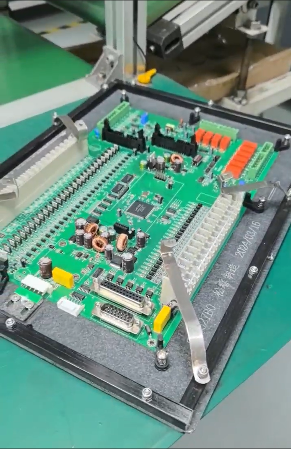
Beyond fabrication, GreatPCB positions itself as a one-stop provider covering PCB fabrication, component sourcing, and assembly. This turnkey structure is designed to reduce the procurement complexity that arises when customers must coordinate multiple vendors—a pain point the company’s Box Build Assembly and Component Sourcing services directly address by integrating sourcing with fabrication and assembly under one process.
Engineering and DFM Support
GreatPCB’s engineering team provides free DFM (Design for Manufacturability) analysis, along with what the company describes as real-world design experience applicable to AI and automotive radar projects. For 5G module developers, this means design feedback can be incorporated before fabrication begins, helping refine layouts for manufacturability and signal performance alike.
Manufacturing Scale and Quality Systems
On the assembly side, GreatPCB uses high-speed pick-and-place equipment from FUJI, PANASONIC, and YAMAHA, supporting SMT, THT, and BGA assembly with reballing. Inspection and testing capability spans AOI, X-Ray, ICT, FCT, and ionic contamination testing—a combination relevant to applications where board delamination and ionic contamination are known risk factors. The company reports a 99% accuracy rate, 97% on-time delivery, and 99% customer satisfaction, alongside a 24-48 hour quick-turn service for FPC and aluminum PCBs.
Quality assurance is further supported by industry certifications including ISO 9001:2015, IATF 16949 (Automotive), UL (ZLPW2), and IPC Class 2/3 compliance. These certifications are particularly relevant for 5G module manufacturers who must also meet automotive or industrial-grade reliability standards in adjacent product lines.
Proven Experience Across Telecommunications-Adjacent Applications
While GreatPCB’s documented customer cases span several industries, two are directly instructive for 5G-related engineering teams. In an automotive radar project at 77GHz, the company applied high-precision PCB design and material stack-up techniques for signal integrity—methods that overlap significantly with the signal integrity demands of 5G RF front-end modules. Separately, in an AI accelerators case for high-performance computing, GreatPCB addressed complex thermal and power design requirements, demonstrating experience with the thermal management challenges that also affect dense 5G infrastructure boards.
Additional case experience includes medical electronics, where high-reliability PCBA met IPC Class 3 standards for life-critical equipment, and flexible electronics, where Flex PCB designs conformed to non-planar surfaces for innovative product form factors. Collectively, these cases indicate a manufacturer whose capabilities extend across signal integrity, thermal management, and high-reliability assembly—three considerations that converge in 5G communication module design.
Choosing a Partner for 5G PCB Fabrication in China
For engineers and procurement managers evaluating China-based manufacturing partners for 5G communication modules, the relevant evaluation criteria typically include material capability (Rogers series, PTFE, ceramic), structural capability (multilayer, HDI, metal core), assembly precision (SMT/BGA with AOI and X-Ray inspection), and the ability to consolidate fabrication, sourcing, and assembly to simplify procurement. GreatPCB’s documented product matrix, equipment base, certification portfolio, and case history across automotive radar, AI accelerators, medical electronics, and flexible electronics together outline a manufacturing profile built to serve the specific technical demands of 5G-era hardware, from initial DFM review through high-volume production.
As 5G deployment continues to scale globally, manufacturers capable of addressing both the RF material science and the thermal/mechanical engineering sides of module design—within a single turnkey relationship—are likely to remain central to how telecommunications hardware teams source their advanced PCB fabrication needs.
Related products
-
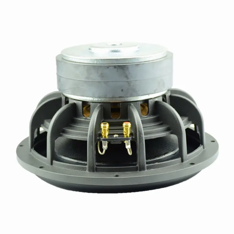
Factory OEM 10 inch large carbon fiber cone woofer subwoofer subwoofer subwoofer speaker home use $72-$79
Contact UsFactory OEM 10 inch big carbon fiber basin woofer speakers super woofer horn super bass loudspeaker subwoofer speaker for home
Factory OEM 10-inch Carbon Fiber Subwoofer (Home Audio) -

Factory 3 inch 4 ohm_8 ohm 15w full range speaker 3 inch full range speaker $2.94-$4.40
Contact Us3″ (76mm) 15W 4Ω Full-Range Multimedia Speaker – Resonant Frequency (F₀): 106Hz, Frequency Response: up to 20kHz
Factory 3 Inch 4Ω/8Ω 15W Full Range Speaker -

DS-RF Selective Formaldehyde module HCHO Module
Contact UsDS-RF selective formaldehyde module can detect HCHO, VOC, TVOC, t & RH at the same time.
-

Foam tape
Contact UsWidely used in electronic and electrical products, mechanical components, various small household appliances, mobile phone accessories
Reviews
There are no reviews yet.